
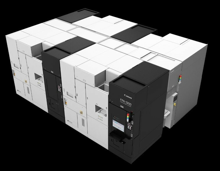
On October 13, 2023, Canon introduced the FPA-1200NZ2C nanoimprint lithography system, an advanced semiconductor manufacturing technology.
Unlike conventional photolithography, which relies on projecting a circuit pattern onto a resist-coated wafer, nanoimprint lithography transfers the circuit by pressing a mask with the desired design onto the resist on the semiconductor wafer, similar to using a die. This unique approach dispenses with an optical mechanism, ensuring that the fine pattern of the circuitry is accurately reproduced from mask to wafer. This allows complex two- or three-dimensional patterns to be created in a single imprint, potentially reducing cost.
In addition, Canon's nanoimprint lithography technology enables patterning on semiconductor devices with a minimum line width of 14nm. This is equivalent to the 5-nm nodes required to produce the most advanced logic semiconductors in existence today. As NIL mask technology continues to evolve, it is expected that circuits with a minimum linewidth of 10 nm, equivalent to a 2 nm node, will be created. This speaks to the incredible precision and innovation of this technology.
In addition to its technical capabilities, the FPA-1200NZ2C system offers environmental advantages. Not needing a specific wavelength light source to create thin circuits significantly reduces power consumption compared to current photolithography equipment (5nm nodes with 15nm line widths). This not only improves energy efficiency, but also reduces carbon dioxide emissions.